|
V. TECHNOLOGY TRENDS ANALYSIS OF INDUSTRY
PWB technology continually evolves the major trends have focused on reducing the size and increasing the capacity of the PWB. These changes are often accomplished through advances in the following technologies: multilayer, surface mounting, fine-pitch, hole density, hole size, and multichip modules.
Using multilayer PWBs (especially high-layer count PWBs) increases capacity and reduces size by allowing more circuitry to be built into one PWB. Each layer has its own circuit pattern. Similarly, using surface-mount technology allows components to be placed on both sides of the PWB instead of just one side, as is the case with through-hole technology. With through-hole mounting, the pins or leads on the component are inserted through holes in the PWB and come out the other side, thereby using up space on that side of the PWB. With surface-mounted components, the pins or leads are attached to pads or lands on one surface of the PWB, so the opposite side of the PWB remains free for either other components or circuitry. A pad or land is the end of a circuit line or trace intended as the connection point for a component. Typically, the pad or land is significantly wider than the rest of the circuit trace in order to approximately match the width of the component lead that will be attached to it.
Pitch refers to the distance from a point on a particular feature to the same point on the adjacent feature. Pitch, as used by the PWB industry, frequently defines the distance from the center of a circuit line (also called "trace") to the center of the adjacent line. The thinner the line and space (or finer the pitch), the more lines can be placed on the PWB. Similarly, density refers to the percentage of the PWB covered by conductors or by components. To save routing space with large-pitch components, PWB designers run circuit lines in-between adjacent pads on which the component leads are mounted. High-density PWBs may have three or more conductors between the pads.
Another technique to reduce size and boost performance is to decrease the size of the vias or holes used to conduct electricity from one side of the PWB to the other or to an inner layer. Finally, another technology for increasing performance while decreasing size is multichip modules (MCMs). For most applications, the bare integrated circuit (IC) chip is sealed in a hermetic or plastic package before being mounted on the PWB. This package protects the IC from moisture and other hazards, but takes up space and increases weight. MCMs consist of multiple bare IC chips mounted directly on a substrate, often quite similar to a small PWB. This MCM can then be coated for protection and used as is as a special type of PWB or mounted on another PWB as part of a larger PWA.
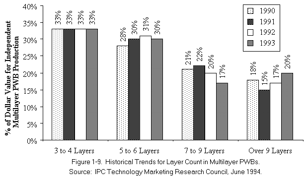
The following information on trends in multilayer technology, as shown in Figure 1-9, refers to the number of different layers used as a percent of all multilayer boards sold. Multilayer PWBs account for about 66% of the market, as discussed in Section IV.B. As evident from Figure 1-9, the relative distribution of three- to four-layer boards has been relatively steady for several years, while that of multilayer boards with nine or more layers has risen slightly over the past three years. In general, however, the production of two- to four-layer boards has declined over the past ten years from approximately 48% of the market in 1984 to 33% of the market in 1993. That decline has been matched by a rise in production of nine plus multilayer boards. The largest markets for multilayer PWBs are computers and communications where size and performance are critical. Consumer products use many single-sided PWBs, because cost is paramount, while size and weight are less critical. For this same reason, the market uses many 1- and 2-sided PWBs.
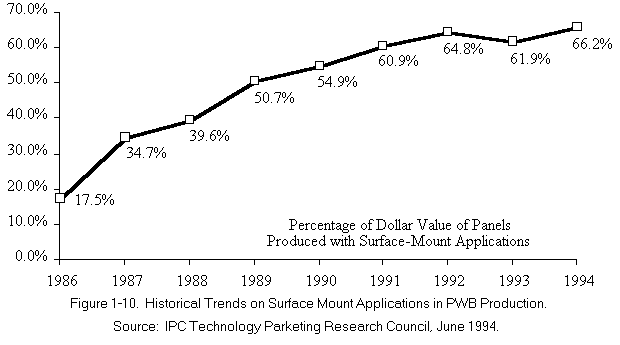
Surface-mount applications (as opposed to through-hole components) save space and allow increased component density on the printed wiring assembly. A history of the growth of surface-mount applications for independent PWB manufacturers is shown in Figure 1-10. In addition to rising surface-mount applications, the percentage of boards with surface-mount applications on both sides of the boards has also been increasing steadily for at least the past seven years, which allows increased performance and decreased size. Of the percentage of all panels with surface-mount applications, the fraction with surface-mount applications on both sides of the panel has increased from about 6% in 1987 to around 21% in 1994. In addition, the percentage of PWBs with 100% surface-mount patterns (i.e., no through-hole components) has increased from about 4% of all panels in 1988 to around 10% of all panels in 1994.
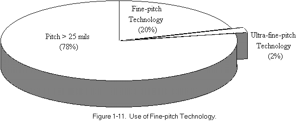
Fine-pitch technology is generally defined as boards with 15 to 25 mils (thousandths of an inch) applications. If the pitch is over 25 mils, then the PWB is not a fine-pitch PWB. Ultra-fine-pitch applications generally refer to applications under 15 mils. The use of fine-pitch technology generally can be traced two ways: historically and by type of PWB manufacturer (OEM vs. independent). With Reference to the former, fine-pitch and ultra-fine-pitch applications have been increasing steadily since the industry began collecting data in 1989. Now, approximately 20% of all PWBs produced have fine-pitch applications, and 45% of surface-mount PWBs have fine-pitch applications. This is approximately double the percentages of five years ago. In addition, ultra-fine-pitch technology is used in about 2% all boards and 4% of surface-mount boards (Figure 1-11). Two factors drive increasing fine- and ultra-fine-pitch technology: the demand for higher performance with reduced size, and increasing technological capabilities that allow fine-pitch PWBs to be produced more reliably.
For this report, the criteria used to measure density applications is the volume of PWB production with a certain number of conductors between lands on 100-mil (0.100") centers (center refers to the center of the land). Density, in this instance, refers to the number of conductors between lands. Thus, a board with no conductors between 100-mil lands is very low density. The data on density production in 1993 is shown in Figure 1-12.
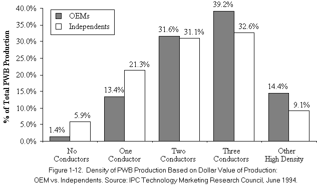
The majority of PWBs produced are medium to high density, with two or three conductors, respectively, between lands. As is often the case, demand for higher performance and smaller size drive higher densities, while cost constraints drive lower densities. High-density PWBs are usually more expensive to produce because of the yields and the greater level of testing that is required (e.g., optical testing of inner layers prior to lamination). The historical trend for density can be summarized as follows: low-density applications (0 to 1 conductors between 100 mil centers) have been steadily declining for approximately 10 years, medium-density boards (2 conductors between 100 mil centers) have remained steady at around 26% to 32%, and high-density applications (3 or more conductors between 100 mil centers) have been steadily increasing over the same time. Thus, the performance/size demands are slowly winning over the cost constraints. At the same time, the technology for producing high-density PWBs has been improving.
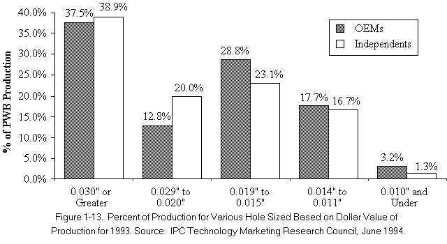
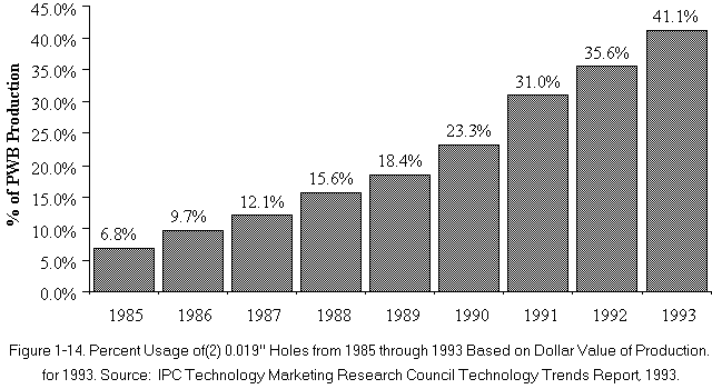
With respect to hole sizes, an overview of percent of production for various hole sizes in 1993 based on dollar value of production is shown in Figure 1-13. In general, use of smaller holes (0.019" or less) has been steadily increasing over the past 10 years from approximately 7% in 1985 to over 40% in 1993 (Figure 1-14). Once again, smaller holes are generally more difficult and expensive to produce, but they do save space.
Platings and coatings on PWBs are primarily used during fabrication for the following purposes: as an etch-resist (typically tin-lead plating); to ensure solderability, typically tin-lead plating or flowed-on solder through HASL (Hot Air Solder Leveling); to protect against moisture or oxidation (often a conformal coating or solder mask); or to mask (cover) certain parts of the PWB against being plated with solder (solder mask). Following are two historical charts on the various types of surface finish and plating or coating techniques used by the PWB industry for the past four years (Figures 1-15 and 1-16).
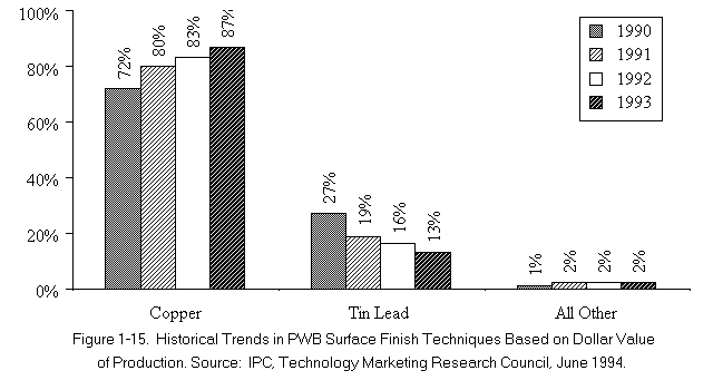
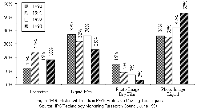
The use of liquid film solder mask and photoimagible dry film solder mask has been generally declining, while the use of photoimagible liquid solder mask has been generally increasing. In addition, for the past four years, the industry has been trying to reduce lead consumption by eliminating tin-lead plating on boards, substituting instead tin plating or organic coatings.
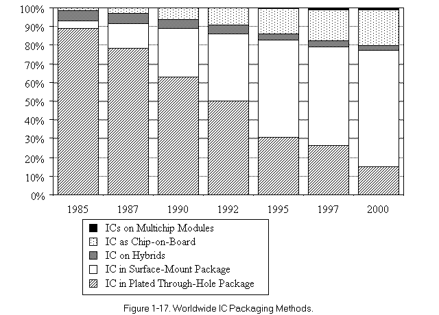
The traditional and still most widely used methods for packaging ICs or "chips" are either surface-mount packages or plated through-hole (PTH) packages. However, in recent years new packaging/assembly methods have been developed, including bare chip attachment methods such as chip-on-board (COB) and MCMs. Although MCMs are still not widely used, this packaging/assembly method is expected to increase in the near future as shown in Figure 1-17.
The advantages of multichip modules include the following:
The three basic MCM types are defined by the type of substrate used and are as follows:
|