|
Printed wiring boards (PWBs) form the basis for interconnecting the devices and components in the vast majority of electronic products. Without this critical component, most electronics products could not function or would be significantly more expensive if constructed with other interconnect technologies. This use-cluster profile will describe the PWB fabrication process for the largest product segment of the industry, the rigid multilayer PWB. The profile focuses on the "subtractive" process, as it is the only broadly implemented approach to fabricating PWBs. Fully "additive" approaches are under development, which would radically change the overall process flow and are described briefly in the Sections I.C.5 and I.C.6.
A use cluster is a set of chemicals, processes, and technologies that can substitute for one another to perform a specific function. A use cluster profile of the PWB industry, therefore, describes alternate chemicals, processes, and technologies that may be used to complete each step or function in the entire PWB manufacturing process.
This use cluster profile is intended to aid in the selection of a use cluster for assessment in a Design for the Environment (DfE) project. The profile identifies different processes in the PWB industry (e.g., laminating, making holes conductive) and steps within those processes (e.g., imaging, etching, plating). The process steps are described in flow chart form with a description of each step. Next, the chemicals, materials, and technologies used in each step are briefly described. The profile may also mention commonly accepted alternatives to these practices, and processes or materials that are recognized to have especially high environmental impacts. Information on the risk and releases of these materials can then be used to target areas for further work.
Printed wiring boards are categorized in several ways. When overall complexity is being considered, they are often categorized in terms of layer-counts, or the number of circuit layers present on a single PWB. PWBs are usually broken down along layer-count lines into three categories: multilayer, double-sided, and single-sided. Multilayer PWBs contain more than two layers of circuitry, i.e., at least one layer is imbedded in the substrate beneath the surface of the board. A multilayer board may consist of 20 or more interconnected layers, but more common are 4, 6, and 8 layers. Double-sided boards have two interconnected layers and are generally easier to produce than multilayer PWBs, while single-sided PWBs have only one layer of circuitry.
PWBs are also categorized by substrate, or base material, type and fall into three basic categories. Rigid PWBs typically are constructed with glass-reinforced epoxy-resin systems that produce a rigid board at thicknesses of less than 0.1" (0.062" is the most common rigid PWB thickness, although there is a trend toward thinner PWBs). Flexible (or flex) circuits are manufactured on polyimide and polyester substrates that remain flexible at finished thicknesses ribbon cables are common flexible circuits. A third category of PWBs consist of boards that are essentially combinations or assemblies of the first two: rigid-flex combinations of one or more rigid PWBs that have one or more flexible circuits laminated to them during the manufacturing process. Three-dimensional circuit assemblies can be created with rigid-flex combinations.
Manufacturing methods can be boiled down to two types, although hybrid methods exist. Most common is subtractive processing, in which copper is selectively removed from a PWB to form a circuit. Within this process, however, copper and other metals are also added during plating steps. The term "subtractive" refers to the method of image transfer from a photo-tool or image file to a copper circuit on a PWB. Additive processing refers to a process in which an image is formed by selectively adding copper (electrolessly plating onto a substrate an image of a circuit). In a fully additive process no etching, or removal of copper, occurs.
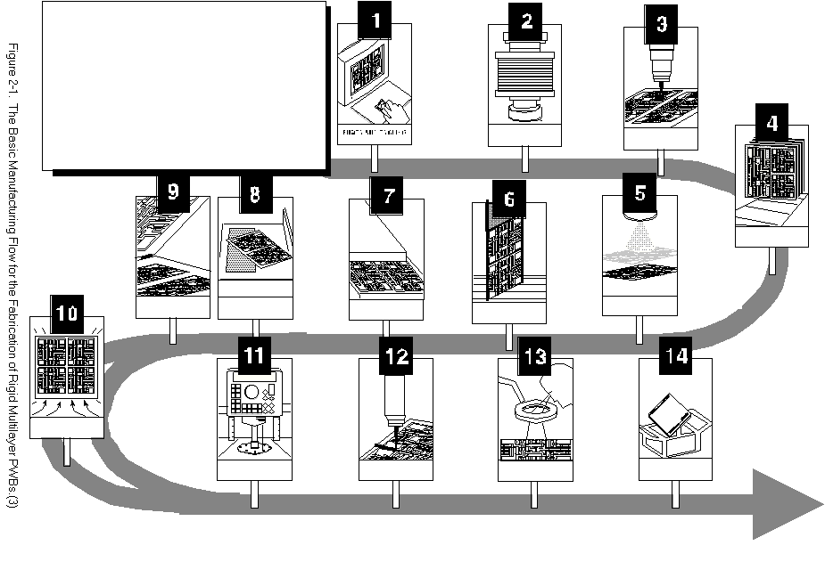
As part of an industry driven activity, the 1994 Electronics Industry Environmental Roadmapb described a generic PWB process, developed in conjunction with the IPC, with comments from technical experts participating in the process (Figure 2-1). Representative of the highest value segment of the PWB market, this process flow is indicative of the manufacture of rigid multilayers. This process description was used as a baseline for selection and definition of the use clusters in this analysis.
Single-sided PWBs continue to be manufactured in high quantities in term of units (71% of PWBs manufactured in the U.S.), but represent only 10% of the total value of U.S. production. Single-sided PWBs are comparatively easy to produce and the market is highly competitive, as demonstrated by the fact that a single-sided PWB costs only about one-tenth that of a double-sided PWB.
Several critical manufacturing steps are not included in the typical single-sided manufacturing sequence and no process is unique to single-sided production. Therefore, any manufacturer of double-sided or multilayer PWBs can produce single-sided ones as well. Few shops produce single-sided panels exclusively, but instead include single-sided PWBs as part of their overall product mix. Many shops do not produce single-sided panels at all due to the market conditions mentioned above.
The most common sequence of single-sided production is drill, print-and-etch, surface finish, and final fabrication. No inner-layer processing is required, and desmear is also eliminated. Furthermore, only in rare cases are plated through-holes required, therefore, the entire cluster of making holes conductive is not applicable to single-sided manufacturers. The holes instead provide mechanical stability for through-hole panels. Drilling may be completely eliminated on single-sided PWBs if the components are all surface-mounted. Alternative methods of single-sided manufacturing are available. For example, for prototyping, single-sided PWBs can be created by selectively milling or routing copper with an NC machine, thereby forming a circuit without using wet processes at all. Other table-top prototype systems have also been devised.
Not unlike single-sided, double-sided PWB manufacturing is also a subset of the multilayer process described in Section II. The inner layer image transfer, lamination, and hole cleaning clusters are not performed. Therefore, any multilayer manufacturer can easily produce double-sided panels and most do so. Double-sided PWBs do require electroless copper or other methods of making holes conductive, since the top and bottom sides of the board require interconnection.
Single- and double-sided manufacturing processes are subsets of the multilayer process. Thus, it is logical to use the multilayer process as the focus of this profile. In addition, multilayer boards represent two-thirds of the overall value of U.S. production dollars, even though they are produced in lower numbers than single- or double-sided PWBs. The rigid multilayer process (rigid PWBs represent about 95% of U.S. production) is discussed in detail in Section II.
A flexible circuit is manufactured on materials that allow for the bending or flexing of the PWB to create a three-dimensional effect. Flex circuits may be designed to be bent into shape once or a few times, or to withstand thousands of flexing cycles. They are found in printers, disk drives, automobile electronics, and a wide range of other common products.
Although similar to rigid manufacturing in many respects, the flexible circuit manufacturing process deals with unique materials and surface finishes, and the process is not integrated into a rigid PWB shop without considerable effort. Therefore, few rigid manufacturers have expanded into the flex market. On the other hand, because an important portion of the flex market is rigid-flex combinations or assemblies, manufacturers of predominantly flex substrates often produce rigid boards as well. Because flexible substrates have larger dimensional tolerances than rigid ones, multilayer flexible circuits are more difficult to manufacture and are less common than rigid multilayer PWBs.
Image transfer, drilling, and through-hole plating are performed in a similar, but not identical manner. Flex substrates are thin and are unlike standard rigid materials some common flex materials are polyimide and polyester, although many others are in use. Thicknesses of only a few mils are common compared with inner-layer rigid material thicknesses of up to 31 mils, and double-sided thicknesses of 62 or more mils. Additionally, tooling and surface finish processes for flexible circuits are quite different from those of rigid PWBs. A cover sheet of similar material to the base film is applied over typical flex circuitry rather than a solder mask and is press laminated over the circuitry. The cover sheet is pre-punched to expose appropriate areas of the circuit for soldering of components and connectors. Not all flex circuits require solder; those that do are hot-air or hot-oil solder-coated. Nickel-gold is also a common finish.
The fabrication of PWBs through the years has relied mainly on a subtractive print and etch process for forming copper conductors. The process flow shown in Figure 2-1 describes such a subtractive approach. In a subtractive process for rigid multilayer PWBs, metal is removed from a solid foil to form the desired interconnect pattern for the inner layers, as shown in Figure 2-2 and described below. The label subtractive comes from the typical processes used for making these inner layers, encompassed in step 2 of the overall process shown in Figure 2-1.
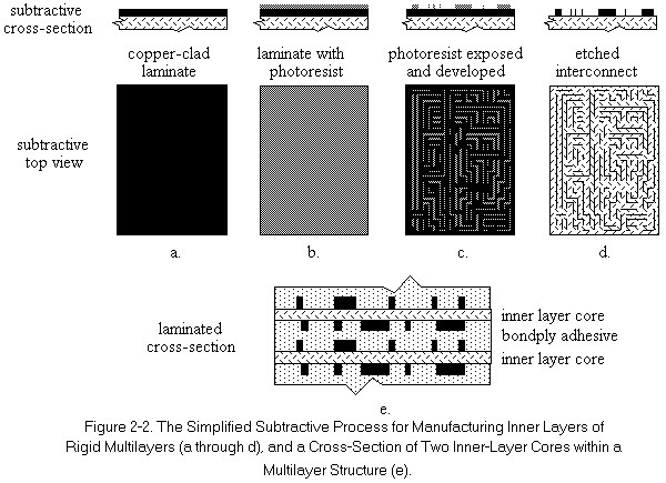
As shown in Figure 2-2, the subtractive process begins with copper-clad laminate, composed of a thin copper foil covering both sides of the epoxy-glass core material (a). The laminate is coated with a sacrificial photopolymer material that acts as a resist in subsequent steps (b). The resist is photoimaged (exposed/developed) to expose the copper to be removed (c). The board is then etched, after which the resist material is stripped and disposed in a fabrication waste stream, leaving the desired interconnect pattern in copper on the exposed laminate (d). In a multilayer structure, each of the inner layers is constructed independently, then laminated together using a B-stage epoxy in between each inner layer core to form the overall structure (e). This non-sequential process of building multilayers is essentially independent of the number of inner layers laminated together and is used to build PWB structures with any number of layers.
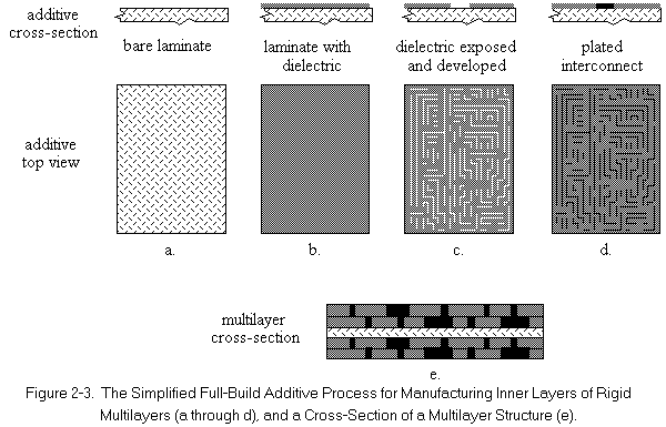
Full-build additive approaches for double- and single-sided boards have been in use for over 20 years. Processes that use full build to make multilayer boards have only recently been under development in this country, and none are in widespread use. Since the additive deposition of seed layers is used for electroplating at certain steps within a subtractive process flow, the full-build descriptor is intended to describe a process where the metal deposition is fully additive, eliminating all etching steps. The intent of these novel approaches is to take advantage of the PWB industry�s current capabilities in photoimaging and printing as used in subtractive processes, while overcoming the limitations and expense of plating, etching, and lamination, as well as eliminating the drilling of vias to form the vertical interconnect between layers.
Each layer is built upon the previous one, so this type of additive approach is also known as a sequential build. As such, there is no lamination step required. Yield considerations become more critical in sequential processing, because an irreparable flaw in the final layer destroys the entire structure. In subtractive processing, the inner layers can be inspected prior to lamination to ensure a higher overall yield.
As shown in Figure 2-3, the additive process for rigid boards begins with a bare catalyzed laminate with no metal on the surfaces (a). Alternatively, with some processes, the first layers on either side of the core laminate are etched to form power and ground planes and may already have plated through-holes. The laminate is coated with a permanent photodielectric material that acts as the dielectric separating the metal layers (b), thus replacing the subsequent core and B-stage layers in the subtractive approach. The dielectric is imaged and developed to form the vias, then a second layer is applied to form the interconnect pattern (c). The board is then selectively plated or metallized by other means, forming the desired interconnect pattern (d). In a multilayer structure, steps (b), (c), and (d) are repeated to form the overall structure (e). In contrast to the conventional subtractive process described previously, this process requires no lamination, with the unreinforced layers built sequentially on the initial rigid core.
Several methods are under consideration for deposition of the circuit traces and vias in an additive structure. None of these methods have been broadly commercialized due to either the maturity, the economics, or outstanding technical challenges. Current research is addressing all of these issues.
The most conventional approach to additive electroless copper plating is to catalyze the entire surface of a bare laminate board by preparing it with liquid solutions containing a latent oxidizer such as ionic tin. Colloidal palladium is applied to the surface and oxidized to the catalytic palladium form. The catalyzed surface is masked using either a temporary or permanent resist. The remaining exposed surface is then plated electrolessly, with the copper adhering only to the exposed catalyzed areas. In some cases photosensitive materials are used to coat a dielectric and then dried to form a catalytic coating. The coating is made selectively catalytic to electroless plating by exposure to light.
The disadvantage of these approaches is that the latent catalyst is left buried under subsequent layers or under any type of permanent resist or dielectric that is used to planarize the circuits. The latent catalyst is a potential source of ionic contamination and possible metal migration and dendritic growth.
In another additive approach, a permanent dry film material is used to build double-sided boards using laminate material with a special catalyst layer. The dry film is laminated, exposed, and developed in the conventional manner and then cured on the board. The exposed catalytic layer is conditioned to expose the catalytic material in it and to provide a better surface for metal adhesion. This is followed by the electroless bath. A process patented and demonstrated by DuPont uses the adhesive characteristics of photopolymers to selectively adhere to metal particles in unexposed areas. The metal particles then catalyze the surface for electroless plating.
One method for image transfer in the fully additive process is screen printing. Screen printing is limited to applications where trace lines are large (>0.008"). In this method, permanent plating resist is printed onto a laminate that either has been or can be made catalytic to electroless plating. The plating resist is screen printed in the reverse image of the circuit lines and copper is plated on the exposed catalyzed laminate. The plating resist is not later etched, but remains as a permanent dielectric. In addition to the fact that this method uses fewer steps and generates less waste, it has the additional advantages of:
The disadvantages of using a screen-printed liquid resist are the following:
Other methods of image transfer used for additive processing include screen printing of conductive polymers and screen printing sinterable metal particles suspended in a polymer matrix. In both of these cases, trace line resistivity is more than one order of magnitude above that of pure copper.
Liquid materials can be used to transfer the actual circuit lines themselves. In these processes, a plating catalyst is bound to a photosensitive material. There are examples of both positive and negative working photosensitive materials systems, although none have been put into volume production. For example, D�Amico and DeAngelo have developed a process called photosensitive metal decomposition (PSMD).d In this case, stannous oxide (SnO) takes one of two reaction paths, depending on whether or not it is exposed to UV light. If exposed, SnO is oxidized to form stannic oxide (SnO2). SnO2 cannot reduce Pd+2 to its metallic form. However, if UV light is not present, then SnO2 in a caustic environment reduces palladium chloride (Pd+2) to palladium (Pd_). Pd_ is a catalyst for electroless copper deposition. Since light is used to prevent catalyst formation and signal line deposition, this process is negative working. As such, it is prone to unwanted copper deposition and shorting due to factors such as particles on the laminate surface or photo-tooling.
Iwaki has developed a process called "photochemical circuits."e In this process, a silver salt is decomposed using ultraviolet light, leaving small sights of reduced silver metal.
This process is positive working since light is used to form the catalyst for electroless metal deposition where exposed. Positive working processes tend to have a higher yield than negative ones. This has been demonstrated in the fabrication of integrated circuits. However, silver is highly mobile and can cause other yield problems because of its mobility. It is also expensive and can form highly unstable salts.
Frisch developed a positive working process called photo formation (PF).f Here, copper metal salt in the form of cupric acetate (CuXX) can be reduced to Cu_ by exposure to UV light. The reaction requires a UV-sensitive reducing agent to be present. The reducing agent, diazoquinone, is also used in photoresists for integrated circuit processing.
Mansfeld and Jans developed a process called physical development-reduction (PDR).g In this process, titanium dioxide (TiO2) particles disbursed into the adhesive are the light-activated reducing agent. A thin layer of Pd+2 is coated over the adhesive. When exposed to UV light, TiO2 is further oxidized and releases electrons that reduce Pd+2 ions to metal form.
Printron, Inc., developed a process called the Printron Process.h In this approach, image transfer can be done via either screen printing (low-density, low-cost) or electrophoretic deposition (high-density and higher costs). This is a positive process where fine solid metal particles are suspended in a proprietary "ink." After the image is transferred in a mode compatible with the cost and density goals, the metal particles are melted using electromagnetic fields. In this way, only the metal is heated. Though promising, this method has not become a dominant product in the market.
One concept under development utilizes a photoimagible dielectric to produce the pattern for vias and interconnect traces. This approach eliminates the need for a separate dielectric and clad metal layer that requires either etching or a combination of plating and etching to produce a circuit. It also eliminates the resist deposition and stripping previously required to define that circuit.
No additional drilling is required to form the vertical interconnect between layers. The connection between layers is formed during the sequential steps described. Any vias desired through the starting core material are formed by conventional drilling and plating techniques prior to the sequential build of interconnect layers.
|